


Copyright � 2016 Altay Inc � All Rights reserved � email: info@kimmonquartz.com
Altay Inc - 1 (855) 717 3932
1010 Oakmead Drive
Arlington, Texas 76011
1010 Oakmead Drive
Arlington, Texas 76011
Welcome to Kimmon Quartz
Altay Inc. is a manufacturer of high purity quartzware made to meet the stringent
requirements of semiconductor fabricators and related industries. We are experienced
with most semiconductor equipment including wet stations, diffusion furnaces, epitaxial
reactors, annealing systems, plasma etchers, ashers, CVD systems and much more. We
routinely fabricate brand new quartz parts for these tools and we also repair broken and
damaged customer supplied quartz parts, revitalizing them to like new condition. Altay�s
manufacturing facility is central located in the Dallas, TX area, just 15 minutes from DFW�s
International Airport.
We aspire to supply precision crafted quartz products at the lowest possible prices!

KimmonQuartz
Your perfect solution!
Your perfect solution!
High Purity Quartzware for Semiconductor Applications
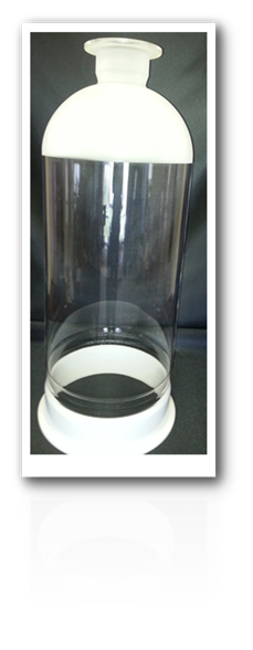
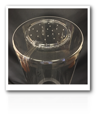
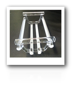
� Diffusion Furnace Tubes, Liners, Pedestals, & Boats
� External Torches, TC Sheaths, Gas Injectors, End Caps, Gas Manifolds,
Manifold Covers
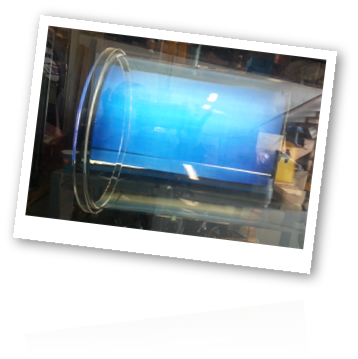
� Quartz Bell Jars for Epitaxial Reactors and HDP (High Density Plasma)
chambers
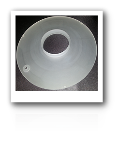
� Quartz fins, adiabatic plates, end effectors, wafer carriers, vacuum wands,
wafer trays
� Equipment process chambers, domes, mini environments
� Wet Bench quartz process baths, megasonics, ultrasonics, heater parts,
mixers, injectors
� Quartz for plasma etch, ash, and CVD systems
� Specialty quartz parts for related industries: solar, pharma, photonics,
substrate manufacturers, Epi foundries, and more.

Products we offer:
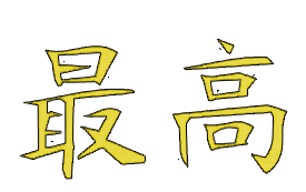
These Japanese characters translate to "Top of the top". The symbols embody a quality ethic that we
adopted years ago when we were called Kimmon Quartz USA. Kimmon remains a great Japanese quartware supplier,
best known for ultra-pure materials crafted with dimensional precision. Altay is the only qualified provider of Kimmon
Quartz in the USA.
We glass blowers use GE Momentive raw starting material. Momentive sets the industry standard for purity. This
material has very low hydroxyl levels due to GE�s unique electrical fusion process. Because of the material�s low
hydroxyl content, Momentive's tubing does not require any specialty coatings. Using high quality starting material is
proven to greatly decrease any undesired devitrification that degrades quartz.
All Altay precision crafted quartzware is final annealed prior to shipment. This final annealing process relieves thermal
stress, eliminates stress related breakage, and ultimately prolongs the part life.
All Altay parts are carefully inspected for compliance to specification including dimensionality, purity, and cosmetics.
Altay Inc. has a long history of semiconductor industry service and our chief glass blower has 30 years of semiconductor
experience.
Quartz Manufacturing Quality Philosophy
High Purity Quartzware for Semiconductor Applications
Diffusion Furnace Tubes, Liners, Pedestals, & Boats
External Torches, TC Sheaths, Gas Injectors, End Caps, Gas Manifolds, Manifold Covers
Quartz Bell Jars for Epitaxial Reactors and HDP (High Density Plasma) chambers
Quartz fins, adiabatic plates, end effectors, wafer carriers, vacuum wands, wafer trays
Equipment process chambers, domes, mini environments
Wet Bench quartz process baths, megasonics, ultrasonics, heater parts, mixers, injectors
Quartz for plasma etch, ash, and CVD systems
Specialty quartz parts for related industries: solar, pharma, photonics, substrate manufacturers, Epi foundries,
and more.